- 您现在的位置:买卖IC网 > Sheet目录1252 > VDRIVE2 (FTDI, Future Technology Devices International Ltd)MOD USB FLASH DRIVE INTERFACE
�� �
�
�2.3� SPI� Interface� Signal� Descriptions� and� Timing� Diagrams�
�Ta?le� 3� -� Data� and� Control� ??us� ?ignal� Mode� ?ptions� -� ??I� Inter?ace�
�Page� �
�Pin� No.�
�?�
�4�
�2�
�6�
�Name�
�?CLK�
�?DI�
�?D?�
�C?�
�Type�
�Input�
�Input�
�?utput�
�Input�
�Description�
�??I� Cloc?� input??� 12MHz� ma?imum.�
�??I� ?erial� Data� Input�
�??I� ?erial� Data� ?utput�
�??I� Chip� ?elect� Input�
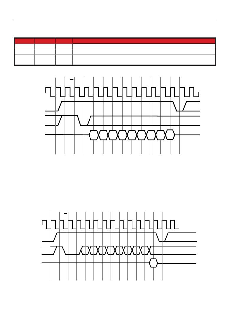
�Figure� 2� -� ??I� ?lave� Data� ?ead� Cycle�
�R/W� ADD� D7�
�D6�
�D5�
�D4�
�D3�
�D2�
�D1�
�D0�
�SPICLK�
�SPI� CS�
�SPI� Data� In�
�1�
�1�
�0�
�SPI� Data� Out�
�From� ?tart� -� ??I� C?� must� ?e� held� high� ?or� the� entire� read� cycle??� and� must� ?e� ta?en� low� ?or� at� least� one� cloc?� period�
�aft?r� th?� r?ad� i?� co??p??t?d.� Th?� fir?t� bit� on� S??I� Data� In� i?� th?� R/W� bit� -� inp?tting� a� ‘1’� h?r?� a??o??� data� to� b?� r?ad� fro??�
�the� chip.� The� ne?t� ?it� is� the� address� ?it??� ?DD??� which� is� used� to� indicate� whether� the� data� register� (?0?)� or� the� status�
�register� (?1?)� is� read� ?rom.� During� the� ??I� read� cycle� a� ?yte� o?� data� will� start� ?eing� output� on� ??I� Data� ?ut� on� the� ne?t�
�c?ock� cyc??� aft?r� th?� addr???� bit??� MSB� fir?t.� ?ft?r� th?� data� ha?� b??n� c?ock?d� o?t� of� th?� chip??� th?� ?tat??� of� S??I� Data�
�?ut� should� ?e� chec?ed� to� see� i?� the� data� read� is� new� data.� ?� ?0?� level� here� on� ??I� Data� ?ut� means� that� the� data� read�
�is� new� data.� ?� ?1?� indicates� that� the� data� read� is� old� data??� and� the� read� cycle� should� ?e� repeated� to� get� new� data.�
�?emem?er� that� C?� must� ?e� held� low� ?or� at� least� one� cloc?� period� ?e?ore� ?eing� ta?en� high� again� to� continue� with� the�
�ne?t� read� or� write� cycle.�
�Figure� 3� -� ??I� ?lave� Data� Write� Cycle�
�R/W� ADD� D7�
�D6�
�D5�
�D4�
�D3�
�D2�
�D1�
�D0�
�SPICLK�
�SPI� CS�
�SPI� Data� In�
�1�
�0�
�0�
�SPI� Data� Out�
�From� ?tart� -� ??I� C?� must� ?e� held� high� ?or� the� entire� write� cycle??� and� must� ?e� ta?en� low� ?or� at� least� one� cloc?� period�
�aft?r� th?� ?rit?� i?� co??p??t?d.� Th?� fir?t� bit� on� S??I� Data� In� i?� th?� R/W� bit� -� inp?tting� a� ‘0’� h?r?� a??o??� data� to� b?� ?ritt?n�
�to� the� chip.� The� ne?t� ?it� is� the� address� ?it??� ?DD??� which� is� used� to� indicate� whether� the� data� register� (?0?)� or� the� status�
�register� (?1?)� is� written� to.� During� the� ??I� write� cycle� a� ?yte� o?� data� can� ?e� input� to� ??I� Data� In� on� the� ne?t� cloc?� cycle�
�aft?r� th?� addr???� bit??� MSB� fir?t.� ?ft?r� th?� data� ha?� b??n� c?ock?d� in� to� th?� chip??� th?� ?tat??� of� S??I� Data� O?t� ?ho??d� b?�
�VDrive2� Vinculum� VNC1L� Module�
�Datasheet� Version� 0.99�
�?� Future� Technology� Devices� International� Ltd.� 2007�
�发布紧急采购,3分钟左右您将得到回复。
相关PDF资料
VDSP-SHARC-PCFLOAT
SOFTWARE VISUALDSP++ FOR SHARC
VDSP-SHARC-PCFLT-5
SOFTWARE SHARC PC FLOAT 5 SEAT
VF2F2
MOD VINCULUM USB DRV DUPLICATOR
VLP190UF
POLYSWITCH PTC RESET 1.9A STRAP
VLP210ULF
POLYSWITCH PTC RESET 2.1A STRAP
VLP270F
POLYSWITCH PTC RESET 2.7A STRAP
VLR170UF
POLYSWITCH PTC RESET 1.7A STRAP
VLR175LF
POLYSWITCH PTC RESET 1.75A STRAP
相关代理商/技术参数
VDRIVE3
功能描述:界面模块 USB Host uController Dev Module Vinculum
RoHS:否 制造商:4D Systems 产品:Serial Converters 通道/端口数量: 数据速率: 接口类型:USB, UART 工作电源电压:3.3 V, 5 V 最大工作温度:
VDRIVE3-LD
制造商:Future Technology Devices International (FTDI Chip) 功能描述:MOD USB FLASH DRV INTRFACE W/LID
VDRS05A014AGE
制造商:Vishay Angstrohm 功能描述:Var MOV 14VAC/18VDC 100A 22V Radial Ammo Pack
VDRS05A014AHE
制造商:Vishay Angstrohm 功能描述:Var MOV 14VAC/18VDC 100A 22V Radial Ammo Pack
VDRS05A014ALE
制造商:Vishay Semiconductors 功能描述:
VDRS05A014AME
制造商:Vishay Angstrohm 功能描述:Var MOV 14VAC/18VDC 100A 22V Radial Ammo Pack
VDRS05A014ASE
制造商:Vishay Angstrohm 功能描述:Var MOV 14VAC/18VDC 100A 22V Radial Ammo Pack
VDRS05A014BFE
制造商:Vishay Semiconductors 功能描述: